Features of our technology
Can you make something like this? Can you do something like that?
We bring such wishes to life.
At Kyosei, our +ONE solution combines precision processing using photo etching technology with a diverse range of other processes to realize unprecedented and innovative shapes and functions.
Technical details
-
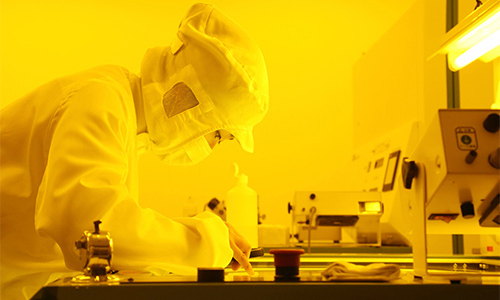
Photoetching core technologyWe offer higher precision and higher density processing than anywhere else, thus contributing to the creation of highly competitive products.
- Half-etching
- Large-format etching
- Special metal etching, and more
-
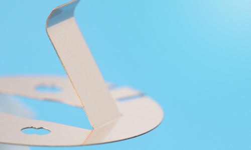
Processing technologyUnique shapes that cannot be created by etching alone can be realized via various processing techniques.
- Diffusion bonding & bonding of dissimilar metals
- Laser welding & spot-welding
- Bending processes
- Grinding, cutting, etc.
-
Surface treatment technologyWhether for decoration or to improve product quality, you can trust our expertise with all kinds of painting and coating.
- Various types of plating
- Black surfacing & black chrome treatment
- Electrolytic polishing & blasting treatment
- Various types of coating
- Mirror surfacing & paint coating processing etc.
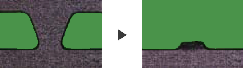
Precision processing
- Processed cross section
-
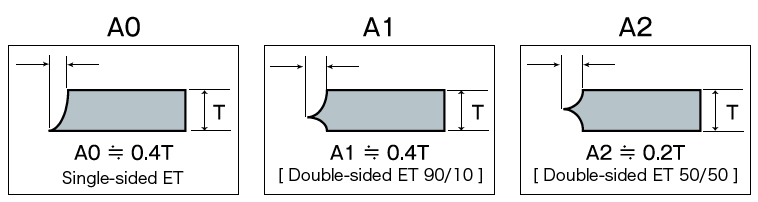
- Processing limits(1)
-
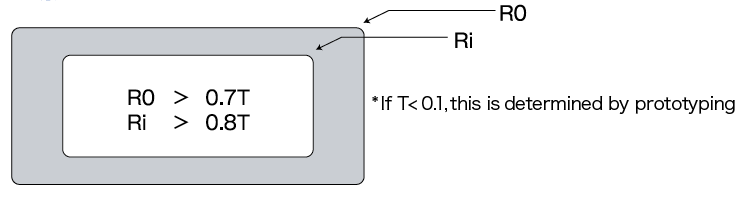
- Processing limits(2)
-
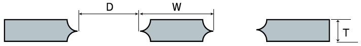
| Thickness (T) | Minimum dimension of D | Practical minimum dimension of D | Practical minimum dimension of W | Precision of DW |
|---|---|---|---|---|
| 5〜12.5 ㎛ | Determined by prototyping | Determined by prototyping | Determined by prototyping | Determined by prototyping |
| 25 ㎛ | ||||
| 50 ㎛ | ≒ 1.6T | 100 ㎛ | ≒ 0.7T | ± 15㎛ |
| 100 ㎛ | ≒ T | 150㎛ | ≒ 0.5T | ± 15㎛ |
| 150 ㎛ | 200 ㎛ | ± 25㎛ | ||
| 250 ㎛ | 250 ㎛ | ± 40㎛ | ||
| 500 ㎛ | 500 ㎛ | ± 75㎛ |
If you require a higher level of precision than listed above, please feel free to consult with us.
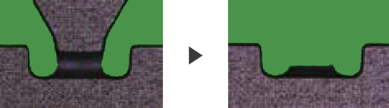
Bridge shapes
Bridge shapes
In the etching process, a bridge is required to connect the product with the frame. Here we present Kyosei’s standard bridge. Our more customized bridges are not posted here due to intellectual property concerns.


Supported materials
Gold, silver, palladium, pure copper, brass, phosphor bronze, BeCu, nickel silver, copper-titanium alloys, SUS, Hastelloy, Inconel, permalloy, Kovar, tungsten, molybdenum, amorphous metals, aluminum, titanium, magnesium, Alloy 42, iron, nickel, and more.
Major fields of application
-
Semiconductor-related componentsSemiconductor test-related components, semiconductor package components, and more.
-

Electronics-related componentsPrecision components for automobiles, smartphones, optical devices, and more.
-
Decor & interiorInterior and exterior design for shops, commercial facilities, automobiles, etc., as well as interior items and more.