Semiconductor-related parts
Products available
Contactors for semiconductor wafers/package inspection, interposers, lead frames for semiconductor packages, lead frames for MEMS semiconductors (various sensors), carrier trays for semiconductor processing, guide plates for semiconductor package sockets, probe card test heads, guide plates and substrate frames for semiconductor devices, and more.
To manufacturers of semiconductors, probe cards, and MEMS:
Are you experiencing any problems with these things?
- You want to make your products smaller, lighter, or thinner.
- You want to create innovative products using unprecedented shapes or materials.
- You want to prototype and mass-produce at low cost.
- You want to create low load contacts.
- You want to apply an insulating treatment between narrow pitches.
- You want to perform multi-pin or narrow pitch drilling.
Your problems can be solved with Kyosei’s photoetching technology.
| With photoetching… |
- Complex and fine processing is possible in micron units
- No burring or distortion caused by processing, giving a beautiful finish
- Can be used for a wide range of metals
- Low costs, small lots, and short delivery times are possible, since metal molds are not required
|
Product Examples
- Contactors for semiconductor wafers/package inspection (spring terminals)
-
- By adding +ONE cutting-edge technology to the etching technology we have cultivated over many years, Kyosei offers test solutions capable of supporting a wide variety of contact methods—from wafer tests to final tests.
- As well as cantilever, vertical, cobra, and MEMS-type probes, Kyosei offers wire probes, probe heads, custom sockets, and probe pins using various barrels, etc.—all of which can be adapted according to client needs from the design stage through to prototyping, evaluation, and mass production.
- In addition to stainless steel, nickel, BeCu, tungsten, and palladium alloys, Kyosei can also process very hard and difficult-to-cut materials (rhodium alloys, aluminum, titanium, magnesium, etc.) that are difficult to process using conventional methods.Supported materials
-
Kyosei offers a variety of surface treatments (gold plating, silver plating, palladium plating, rhodium plating, DLC coating, insulating treatments, black oxide treatments, GD coatings, and more).

- In addition to flat etching, 3D etching can also be performed on metal materials such as pipe materials or wire/bar materials. We can perform spiral etching on pipe materials to create spring forms, as well as etching slits or grooves, tip processing for extremely fine wire, and secondary laser processing.
- Using the etching process, high-quality contactors can be achieved without the machining burrs commonly found with mechanical machining (cutting, grinding, etc.) or press processing using dies.
- Lead frame for semiconductor packages
-
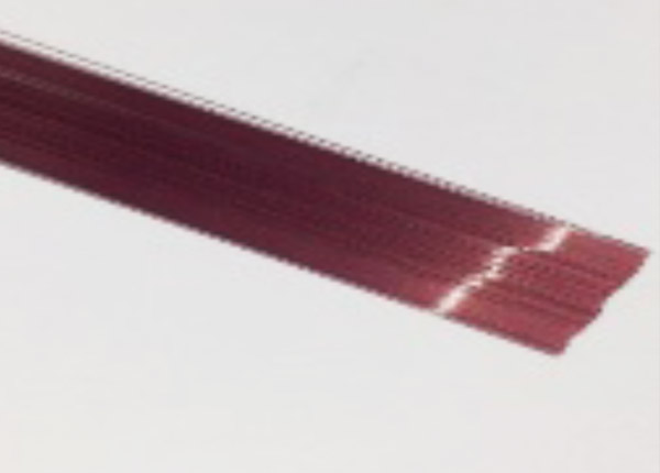
Etching processes can be used for lead frames. Mass production (quality, cost, delivery times) is available at our Thailand factory. Can also be used for ultra-fine SUS materials as thin as 0.004 mm.
- MEMS semiconductor packages
-
We carry out allocation designs to maximize the number of products handled. Etching in any material form (sheets, rolls) is supported.
- Carrier/shipping trays for semiconductor processing
-
Three-dimensional shapes for carrier trays can be handled in-house by joining plates (laser welding). We have a proven record for manufacturing various kinds of trays from bonded products obtained by stacking multiple layers of 3mm SUS material.
- Test heads and guide plates for probe cards/IC sockets
-
As an alternative to resin-drilled products, this can be applied to insulation-treated items for etching workpieces in metal materials. We offer insulated-treated parts as guide plates for thin plate-etched products with multiple holes and narrow pitches. Besides round holes, hex-shaped holes and rectangular holes are also available.
- Guide plates and substrate frames for semiconductor devices
-
Supports products processed with multiple punch holes and products that require modification to be more lightweight. We offer etching mesh processing with SUS materials changed to aluminum or magnesium.
-
- Interposers for probe cards
-
This is the Kyosei difference.
- Smaller, finer, and thinner than anywhere else
- We offer etching processes at a thickness of 0.004 mm (among the thinnest in the world).
- Wide range of supported materials and hardness
- We can tailor the ideal solution to your purpose and applications.
- Ability to deliver innovation
- We developed the industry’s first high conductivity/low load spring.
- High quality × low cost × short delivery time
- Prototypes delivered as fast as 3 days. Low-cost mass production with Japanese-built quality is also possible.
- Responsive support
- Support from specialists in every field. We can also consult on structural design.


